POWER5
 POWER5 MCM | |
| General information | |
|---|---|
| Launched | 2004 |
| Designed by | IBM |
| Performance | |
| Max. CPU clock rate | 1.5 GHz to 2.3 GHz |
| Cache | |
| L1 cache | 32+32 KB/core |
| L2 cache | 1.875 MB/chip |
| L3 cache | 36 MB/chip (off-chip) |
| Architecture and classification | |
| Technology node | 130 nm to 90 nm |
| Instruction set | PowerPC 2.02 |
| Physical specifications | |
| Cores |
|
| History | |
| Predecessor | POWER4 |
| Successor | POWER6 |
| POWER, PowerPC, and Power ISA architectures |
|---|
| NXP (formerly Freescale and Motorola) |
| IBM |
|
| IBM/Nintendo |
| Other |
| Related links |
| Cancelled in gray, historic in italic |


The POWER5 is a microprocessor developed and fabricated by IBM. It is an improved version of the POWER4. The principal improvements are support for simultaneous multithreading (SMT) and an on-die memory controller. The POWER5 is a dual-core microprocessor, with each core supporting one physical thread and two logical threads, for a total of two physical threads and four logical threads.
History
[edit]Technical details of the microprocessor were first presented at the 2003 Hot Chips conference. A more complete description was given at Microprocessor Forum 2003 on 14 October 2003. The POWER5 was not sold openly and was used exclusively by IBM and their partners. Systems using the microprocessor were introduced in 2004. The POWER5 competed in the high-end enterprise server market, mostly against the Intel Itanium 2 and to a lesser extent, the Sun Microsystems UltraSPARC IV and the Fujitsu SPARC64 V. It was superseded in 2005 by an improved iteration, the POWER5+.
Description
[edit]The POWER5 is a further development of the POWER4. The addition of two-way multithreading required the duplication of the return stack, program counter, instruction buffer, group completion unit and store queue so that each thread may have its own. Most resources, such as the register files and execution units, are shared, although each thread sees its own set of registers. The POWER5 implements simultaneous multithreading (SMT), where two threads are executed simultaneously. The POWER5 can disable SMT to optimize for the current workload.
As many resources such as the register files are shared by two threads, they are increased in capacity in many cases to compensate for the loss of performance. The number of integer and floating-point registers is increased to 120 each, from 80 integer and 72 floating-point registers in the POWER4. The floating-point issue queue is also increased in capacity to 24 entries from 20. The capacity of the L2 unified cache was increased to 1.875 MB and the set-associativity to 10-way. The unified L3 cache was brought on-package instead of located externally in separate chips. Its capacity was increased to 36 MB. Like the POWER4, the cache is shared by the two cores. The cache is accessed via two unidirectional 128-bit buses operating at half the core frequency.
The on-die memory controller supports up to 64 GB of DDR and DDR2 memory. It uses high-frequency serial buses to communicate with external buffers that interface the dual inline memory modules (DIMMs) to the microprocessor.
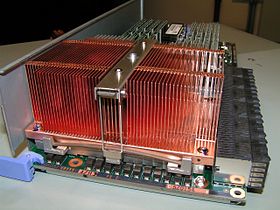
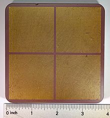
The POWER5 contains 276 million transistors and has an area of 389 mm2. It is fabricated by IBM in a 0.13 μm silicon on insulator (SOI) complementary metal–oxide–semiconductor (CMOS) process with eight layers of copper interconnect. The POWER5 die is packaged in either a dual chip module (DCM) or a multi-chip module (MCM). The DCM contains one POWER5 die and its associated L3 cache die. The MCM contains four POWER5 dies and four L3 cache dies, one for each POWER5 die, and measures 95 mm by 95 mm.[1][2]
Several POWER5 processors in high-end systems can be coupled together to act as a single vector processor by a technology called ViVA (Virtual Vector Architecture).
POWER5+
[edit]The POWER5+ is an improved iteration of the POWER5 introduced on 4 October 2005. Improvements initially were lower power consumption, due to the newer process it was fabricated in. The POWER5+ chip uses a 90 nm fabrication process. This resulted in the die size decrease from 389 mm2 to 243 mm2.
Clock frequency was not increased at launch and remained between at 1.5 to 1.9 GHz. On 14 February 2006, new versions raised the clock frequency to 2.2 GHz and then to 2.3 GHz on 25 July 2006.
The POWER5+ was packaged in the same packages as previous POWER5 microprocessors, but was also available in a quad-chip module (QCM) containing two POWER5+ dies and two L3 cache dies, one for each POWER5+ die. These QCM chips ran at a clock frequency of between 1.5 and 1.8 GHz.
Products
[edit]IBM uses the DCM and MCM POWER5 microprocessors in its System p and System i server families, in its DS8000 storage server, and as embedded microprocessors in its high-end Infoprint printers. DCM POWER5 microprocessors are used by IBM in its high-end IntelliStation POWER 285 workstation. Third-party users of POWER5 microprocessors are Groupe Bull, in its Escala servers, and Hitachi, in its SR11000 computers with up to 128 POWER5+ microprocessors, which have several installations featured in the 2007 TOP500 list of supercomputers. IBM uses the POWER5+ QCM in its System p5 510Q, 520Q, 550Q and 560Q servers.[3]
Notes
[edit]- ^ Glaskowsky, "IBM Raises Curtain on Power5".
- ^ Krewell, "Power5 Tops On Bandwidth".
- ^ IBM System p5 Quad-Core Module Based on POWER5+ Technology: Technical Overview and Introduction
See also
[edit]References
[edit]- "IBM Previews Power5". (8 September 2003). Microprocessor Report.
- Clabes, Joachim et al. (2004). "Design and Implementation of the POWER5 Microprocessor". Proceedings of 2004 IEEE International Solid-State Circuits Conference.
- Glaskowsky, Peter N. (14 October 2003). "IBM Raises Curtain on Power5". Microprocessor Report.
- Kalla, Ron; Sinharoy, Balaram; Tendler, Joel M. (2004). "IBM Power5 Chip: A Dual-Core Multithreaded Processor". IEEE Micro.
- Krewell, Kevin (22 December 2003). "Power5 Tops On Bandwidth". Microprocessor Report.
- Sinharoy, Balaram et al. (2005). "POWER5 System Microarchitecture". IBM Journal of Research and Development.
- Vance, Ashlee (4 October 2005). "IBM pumps Unix line full of Power5+". The Register.
External links
[edit]- Sizing up the Super Heavyweights, a comparison and analysis of the POWER5 and Montecito, that explains the major changes between the POWER4 to the POWER5, along with performance estimates
- A High-Performance IBM Power5+ p5-575 Cluster 1600 and DDN S2A9550 Storage, Texas A&M University
